- 您现在的位置:买卖IC网 > Sheet目录3861 > PIC18F26K80-I/MM (Microchip Technology)MCU PIC 64KB FLASH 28QFN
PIC18F66K80 FAMILY
DS39977F-page 260
2010-2012 Microchip Technology Inc.
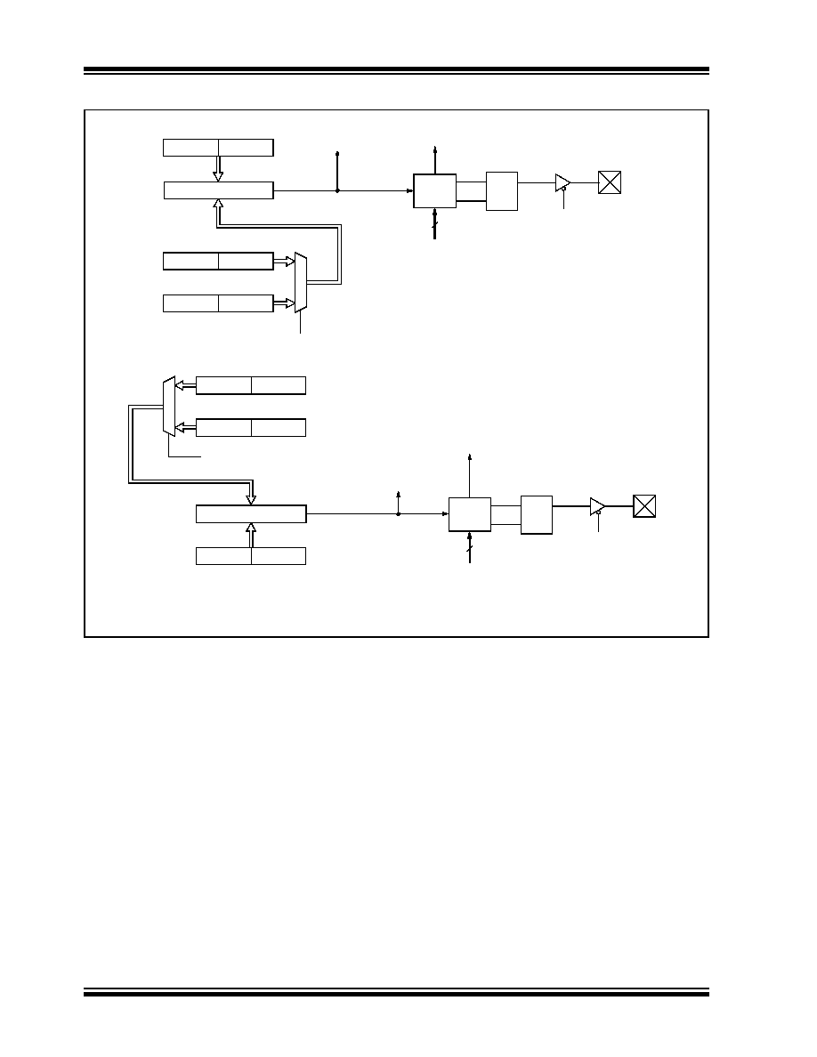
FIGURE 19-2:
COMPARE MODE OPERATION BLOCK DIAGRAM
CCPR5H
CCPR5L
TMR1H
TMR1L
Comparator
Q
S
R
Output
Logic
Special Event Trigger
Set CCP5IF
CCP5 Pin
TRIS
CCP5CON<3:0>
Output Enable
TMR3H
TMR3L
1
0
Compare
4
(Timer1/3 Reset)
Match
Note:
This block diagram uses CCP4 and CCP5, and their appropriate timers as an example. For details on all of
the CCP modules and their timer assignments, see Table 19-2.
TMR1H
TMR1L
TMR3H
TMR3L
CCPR4H
CCPR4L
Comparator
C4TSEL
Set CCP4IF
1
0
Q
S
R
Output
Logic
Special Event Trigger
CCP4 Pin
TRIS
CCP4CON<3:0>
Output Enable
4
(Timer1/Timer3 Reset)
Compare
Match
C5TSEL
发布紧急采购,3分钟左右您将得到回复。
相关PDF资料
PIC16C55-RC/P
IC MCU OTP 512X12 28DIP
SFW23R-2STE1
SFW23R-2STE1-FFC/FPC CONN
PIC24FJ64GA002-E/SS
IC PIC MCU FLASH 64K 28-SSOP
PIC18LF46K22-I/ML
IC PIC MCU 64KB FLASH 44QFN
PIC18F45K80-I/ML
MCU PIC 32KB FLASH 44QFN
PIC24F32KA302-I/ML
MCU 32KB FLASH 2KB RAM 28-QFN
PIC18LF45K80-I/ML
MCU PIC ECAN 32KBFLASH 44QFN
PIC18F4221-I/PT
IC PIC MCU FLASH 2KX16 44TQFP
相关代理商/技术参数
PIC18F26K80-I/SO
功能描述:8位微控制器 -MCU 64KB FL 4KBRM 16MIPS 12bit ADC CTMU RoHS:否 制造商:Silicon Labs 核心:8051 处理器系列:C8051F39x 数据总线宽度:8 bit 最大时钟频率:50 MHz 程序存储器大小:16 KB 数据 RAM 大小:1 KB 片上 ADC:Yes 工作电源电压:1.8 V to 3.6 V 工作温度范围:- 40 C to + 105 C 封装 / 箱体:QFN-20 安装风格:SMD/SMT
PIC18F26K80-I/SP
功能描述:8位微控制器 -MCU 64KB FL 4KBRM 16MIPS 12bit ADC CTMU RoHS:否 制造商:Silicon Labs 核心:8051 处理器系列:C8051F39x 数据总线宽度:8 bit 最大时钟频率:50 MHz 程序存储器大小:16 KB 数据 RAM 大小:1 KB 片上 ADC:Yes 工作电源电压:1.8 V to 3.6 V 工作温度范围:- 40 C to + 105 C 封装 / 箱体:QFN-20 安装风格:SMD/SMT
PIC18F26K80-I/SS
功能描述:8位微控制器 -MCU 64KB FL 4KBRM 16MIPS 12bit ADC CTMU RoHS:否 制造商:Silicon Labs 核心:8051 处理器系列:C8051F39x 数据总线宽度:8 bit 最大时钟频率:50 MHz 程序存储器大小:16 KB 数据 RAM 大小:1 KB 片上 ADC:Yes 工作电源电压:1.8 V to 3.6 V 工作温度范围:- 40 C to + 105 C 封装 / 箱体:QFN-20 安装风格:SMD/SMT
PIC18F26K80T-I/ML
功能描述:8位微控制器 -MCU 64KB FL 4KBRM 16MIPS 12bit ADC CTMU RoHS:否 制造商:Silicon Labs 核心:8051 处理器系列:C8051F39x 数据总线宽度:8 bit 最大时钟频率:50 MHz 程序存储器大小:16 KB 数据 RAM 大小:1 KB 片上 ADC:Yes 工作电源电压:1.8 V to 3.6 V 工作温度范围:- 40 C to + 105 C 封装 / 箱体:QFN-20 安装风格:SMD/SMT
PIC18F26K80T-I/MM
功能描述:8位微控制器 -MCU ECAN 64KB FL 4KBRM 16 MIPS 12b ADC CTMU RoHS:否 制造商:Silicon Labs 核心:8051 处理器系列:C8051F39x 数据总线宽度:8 bit 最大时钟频率:50 MHz 程序存储器大小:16 KB 数据 RAM 大小:1 KB 片上 ADC:Yes 工作电源电压:1.8 V to 3.6 V 工作温度范围:- 40 C to + 105 C 封装 / 箱体:QFN-20 安装风格:SMD/SMT
PIC18F26K80T-I/SO
功能描述:8位微控制器 -MCU 64KB FL 4KBRM 16MIPS 12bit ADC CTMU RoHS:否 制造商:Silicon Labs 核心:8051 处理器系列:C8051F39x 数据总线宽度:8 bit 最大时钟频率:50 MHz 程序存储器大小:16 KB 数据 RAM 大小:1 KB 片上 ADC:Yes 工作电源电压:1.8 V to 3.6 V 工作温度范围:- 40 C to + 105 C 封装 / 箱体:QFN-20 安装风格:SMD/SMT
PIC18F26K80T-I/SS
功能描述:8位微控制器 -MCU 64KB FL 4KBRM 16MIPS 12bit ADC CTMU RoHS:否 制造商:Silicon Labs 核心:8051 处理器系列:C8051F39x 数据总线宽度:8 bit 最大时钟频率:50 MHz 程序存储器大小:16 KB 数据 RAM 大小:1 KB 片上 ADC:Yes 工作电源电压:1.8 V to 3.6 V 工作温度范围:- 40 C to + 105 C 封装 / 箱体:QFN-20 安装风格:SMD/SMT
PIC18F27J13-I/ML
功能描述:8位微控制器 -MCU 128KB Flash 4KB RAM 12MIPS nanoWatt RoHS:否 制造商:Silicon Labs 核心:8051 处理器系列:C8051F39x 数据总线宽度:8 bit 最大时钟频率:50 MHz 程序存储器大小:16 KB 数据 RAM 大小:1 KB 片上 ADC:Yes 工作电源电压:1.8 V to 3.6 V 工作温度范围:- 40 C to + 105 C 封装 / 箱体:QFN-20 安装风格:SMD/SMT